6
LTC4210-1/LTC4210-2
421012f
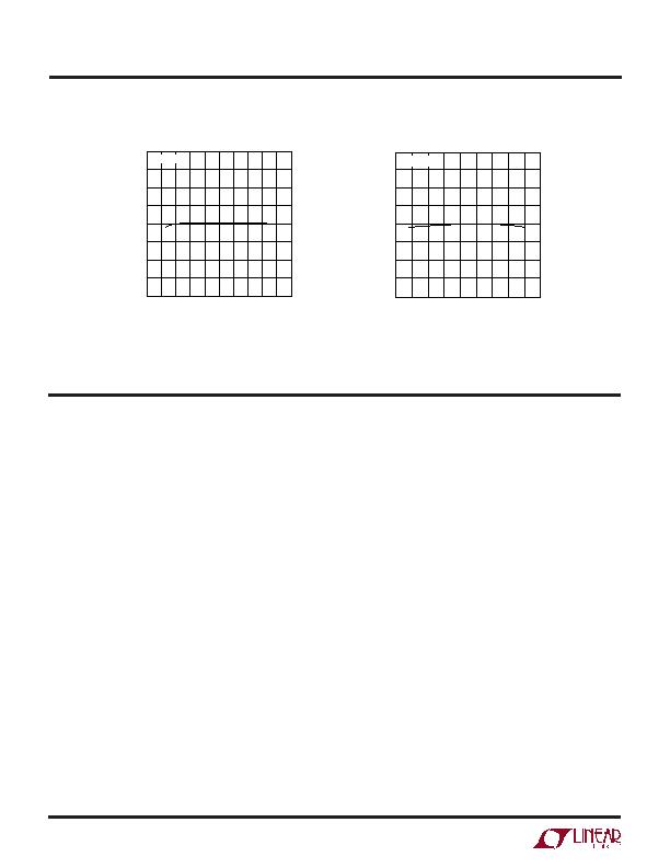
V
CB
vs Supply Voltage
4210 G24
SUPPLY VOLTAGE (V)
0
58
56
54
52
50
48
46
44
42
16
4
2
6
10
14
18
8
12
20
58
56
54
52
50
48
46
44
42
T
A
= 25癈
75
150
25
50
0 25 50 75 100 125
TEMPERATURE (癈)
4210 G25
V
CC
= 5V
TYPICAL PERFOR A CE CHARACTERISTICS
W
V
CB
vs Temperature
U
U
PI FU CTIO S
TIMER (Pin 1): Timer Input Pin. An external capacitor
C
TIMER
sets a 272.9ms/礔 initial timing delay and a 21.7ms/
礔 circuit breaker delay. The GATE pin turns off whenever
the TIMER pin is pulled beyond the COMP2 threshold,
such as for overvoltage detection with an external zener.
GND (Pin 2): Ground Pin.
ON (Pin 3): ON Input Pin. The ON pin comparator has a
low-to-high threshold of 1.3V with 80mV hysteresis and a
glitch filter. When the ON pin is low, the LTC4210 is reset.
When the ON pin goes high, the GATE turns on after the
initial timing cycle.
GATE (Pin 4): GATE Output Pin. This pin is the high side
gate drive of an external N-channel MOSFET. An internal
charge pump provides a 10礎 pull-up current with Zener
clamps to V
CC
and ground. In overload, the error amplifier
(EA) controls the external MOSFET to maintain a constant
load current. An external R-C compensation network
should be connected to this pin for current limit loop
stability.
SENSE (Pin 5): Current Limit Sense Input Pin. A sense
resistor between the V
CC
and SENSE pins sets the analog
current limit. In overload, the EA controls the external
MOSFET gate to maintain the SENSE pin voltage at 50mV
below V
CC
. When the EA is maintaining current limit, the
TIMER circuit breaker mode is activated. The current limit
loop/circuit breaker mode can be disabled by connecting
the SENSE pin to the V
CC
pin.
V
CC
(Pin 6): Positive Supply Input Pin. The operating
supply voltage range is between 2.7V to 16.5V. An under-
voltage lockout (UVLO) circuit with a glitch filter resets the
LTC4210 when a low supply voltage is detected.
发布紧急采购,3分钟左右您将得到回复。
相关PDF资料
LTC4211IMS8
IC CONTROLLER HOT SWAP 8-MSOP
LTC4212IMS#TRPBF
IC CTRLR HOTSWAP TIMEOUT 10MSOP
LTC4214-1IMS#TRPBF
IC CTRLR HOTSWAP NEGVOLT 10MSOP
LTC4215IUFD#PBF
IC CNTRLR HOT SWAP 24-QFN
LTC4216IDE#TRPBF
IC CNTRLR HOT SWAP 12-DFN
LTC4221IGN#TRPBF
IC CTRLR HOTSWAP DUAL 16SSOP
LTC4222CG#PBF
IC CTRLR DUAL HOT SWAP 36-SSOP
LTC4223CDHD-2#PBF
IC CNTRLR HOT SWAP DUAL 16-DFN
相关代理商/技术参数
LTC4210-2CS6#TRMPBF
功能描述:IC CONTROLLER HOT SWAP TSOT23-6 RoHS:是 类别:集成电路 (IC) >> PMIC - 热交换 系列:- 标准包装:50 系列:- 类型:热交换控制器 应用:-48V 远程电力系统,AdvancedTCA ? 系统,高可用性 内部开关:无 电流限制:可调 电源电压:11.5 V ~ 14.5 V 工作温度:-40°C ~ 85°C 安装类型:表面贴装 封装/外壳:10-TFSOP,10-MSOP(0.118",3.00mm 宽) 供应商设备封装:10-MSOP 包装:管件
LTC4210-2CS6#TRPBF
功能描述:IC CONTROLLER HOT SWAP TSOT23-6 RoHS:是 类别:集成电路 (IC) >> PMIC - 热交换 系列:- 标准包装:50 系列:- 类型:热交换控制器 应用:-48V 远程电力系统,AdvancedTCA ? 系统,高可用性 内部开关:无 电流限制:可调 电源电压:11.5 V ~ 14.5 V 工作温度:-40°C ~ 85°C 安装类型:表面贴装 封装/外壳:10-TFSOP,10-MSOP(0.118",3.00mm 宽) 供应商设备封装:10-MSOP 包装:管件
LTC4210-2IS6
制造商:LINER 制造商全称:Linear Technology 功能描述:Hot Swap Controller in 6-Lead SOT-23 Package
LTC4210-2IS6#PBF
制造商:Linear Technology 功能描述:HOT SWAP CNTRL INT SWITCH 6T 制造商:Linear Technology 功能描述:HOT SWAP CNTRL, INT SWITCH, 6TSOT23 制造商:Linear Technology 功能描述:HOT SWAP CONTROLLER, 2.7-16.5V, TSOT-23-6; Controller Applications:Electronic Circuit Breaker, Hot Board Insertion, Industrial High Side Switch / Circuit Breaker; Internal Switch:Yes; Supply Voltage Min:2.7V; Supply Voltage Max:16.5V;RoHS Compliant: Yes
LTC4210-2IS6#TR
功能描述:IC CONTROLLER HOT SWAP TSOT23-6 RoHS:否 类别:集成电路 (IC) >> PMIC - 热交换 系列:- 标准包装:50 系列:- 类型:热交换控制器 应用:-48V 远程电力系统,AdvancedTCA ? 系统,高可用性 内部开关:无 电流限制:可调 电源电压:11.5 V ~ 14.5 V 工作温度:-40°C ~ 85°C 安装类型:表面贴装 封装/外壳:10-TFSOP,10-MSOP(0.118",3.00mm 宽) 供应商设备封装:10-MSOP 包装:管件
LTC4210-2IS6#TRM
制造商:Linear Technology 功能描述:Hot Swap Controller 1-CH 16.5V 6-Pin TSOT-23 T/R
LTC4210-2IS6#TRMPBF
功能描述:IC CONTROLLER HOT SWAP TSOT23-6 RoHS:是 类别:集成电路 (IC) >> PMIC - 热交换 系列:- 标准包装:50 系列:- 类型:热交换控制器 应用:-48V 远程电力系统,AdvancedTCA ? 系统,高可用性 内部开关:无 电流限制:可调 电源电压:11.5 V ~ 14.5 V 工作温度:-40°C ~ 85°C 安装类型:表面贴装 封装/外壳:10-TFSOP,10-MSOP(0.118",3.00mm 宽) 供应商设备封装:10-MSOP 包装:管件
LTC4210-2IS6#TRPBF
功能描述:IC CONTROLLER HOT SWAP TSOT23-6 RoHS:是 类别:集成电路 (IC) >> PMIC - 热交换 系列:- 标准包装:50 系列:- 类型:热交换控制器 应用:-48V 远程电力系统,AdvancedTCA ? 系统,高可用性 内部开关:无 电流限制:可调 电源电压:11.5 V ~ 14.5 V 工作温度:-40°C ~ 85°C 安装类型:表面贴装 封装/外壳:10-TFSOP,10-MSOP(0.118",3.00mm 宽) 供应商设备封装:10-MSOP 包装:管件
